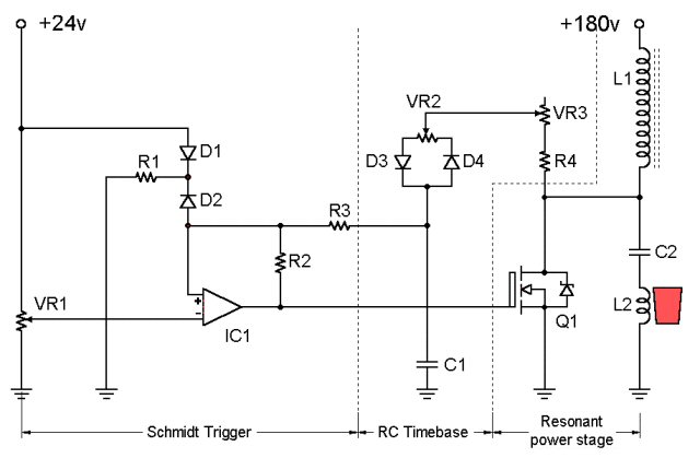
A conceptual MOSFET self resonant oscillator
This design is a result of small scale experimentation. I originally
wanted to use SCRs because of the simplicity of the design. But it
turns out that low cost, readily available SCRs do not handle a
frequency high enough to heat small crucibles full of metal, nothing
above 10KHz. My application induction of heating requires frequencies
between 200kHz and 1Mhz. So I turned to MOSFET devices and a self
resonant circuit made the most sense.Please note that this circuit is conceptual only. Please do not email
me asking for part numbers and component values. They will not do you
any good! I have experimented using small devices, and because the
circuit is still under development, you should not take this
information as how-to! This page is here only to detail my research,
experiments, and observations.
UPDATE: October 2011 — I found this site: http://www.rmcybernetics.com/projects/DIY_Devices/diy-induction-heater.htm which is very much along the same thoughts of being self-resonant. Why didn’t I think of this?? I remember these royer circuits from the Radio Shack experimenters kits, they were simple and easy to build with many variations and sizes/shapes if you will. The link above is a royer with big power mosfets instead of the 2SA transistors that the RS 160-in-1 had. Great idea. Great job, RM Cybernetics.
Below is my understanding and explanation of the circuit’s operation.
For those of you who know more about induction heating than I do,
please send me your comments!
Here’s what I observed in a similar concept circuit on my Phillips 35MHz oscilloscope.The
circuit was running on 12 volts. The top trace was taken at the drain
lead on the MOSFET (I was using an IRF510 at this particular moment)
which is also the connection between L1 and C2. Basically it represents
the charge on C2.
The bottom trace was taken at the connection between C2 and L2. It
represents the voltage across L2. Following is an explanation of how
this circuit works.
When the circuit is powered up, a charge gradually builds in timing
capacitor C1. When it exceeds the reference voltage set by VR1, the op
amp’s output snaps up and closes Q1. This rapid change sets up a
‘ringing’ in the resonant power stage. The positive half of this ‘ring’
is conducted by Q1 itself, and the negative half is conducted by Q1’s
intrinsic diode (gotta love them MOSFET’s!). In the oscillogram, note
only one complete cycle occurs.
During this resonant state, some other things are happening. Full power
supply voltage is drawn across inductor L1 while Q1 is closed. This
builds up flux in L1, which then releases a spike of energy into C2
when Q1 opens. This spike is seen on the oscillogram on the top trace
as a sloping signal.
Also, while Q1 is closed, the voltage on C1 is drained, and when it
drops below the reference set by VR1, the op amp’s output snaps back
low, opening Q1 and letting L1 yank C2 back up to about 1.5 times the
power supply voltage. This rise is timed by C1, and the cycle repeats.
What we ultimately want to achieve is a high voltage, high amperage,
high frequency alternating current (‘ringing’) in L2, which is the work
coil. This will induce currents in a mass of metal, heating it and
ultimately melting it. The industry has this principle perfected for
industrial use, and my goal is to develop a circuit applicable to home
shop use.
 Waveform in MOSFET self resonant circuit
NEWS FLASH!! For all of you
waiting with bated breath for progress on this page, I have revised my
concept circuit. First I will go over the fundamental differences
between this and the original concept circuit:First, the R/C timebase gets its signal from a current sensor rather
than a voltage sensor. This is the main difference. Resistor R1 is a
very low resistance, in the milliohms, like an ammeter shunt. 30-50
amps across this resistor will only draw a voltage drop around 1 volt.
The negative supply to the op amps will probably be -5 volts, to give
them a good operating margin.
This current sensing method to charge and discharge timing capacitor C1
means that the oscillating frequency of the circuit is proportional to
(a) the inductance of L1 and L2, and (b) the resistive load presented
to inductor L2.
The frequency (read: power draw) can be tuned by adjusting variable
resistor VR. Moving the wiper on VR to the right will cause the
frequency to be higher, and power draw to be less. Moving to the left
will cause Q1’s on-state to be longer, making a lower frequency, and a
higher power draw. R3 and R4 simply set the upper and lower limits of
the “gain” of the Sensing Preamp stage of the circuit. These values are
not established yet.
This circuit presents a “convenience” over the previous: Because the
charging and discharging of RC Timebase capacitor C1 follows the RMS or
“area under curve” value of the amperage through (and resulting voltage
across) shunt resistor R1, the current draw of the circuit will be
constant regardless of the inductance values of L1 and L2. The
convenience is the ability to operate the circuit with a variety of
inductances and frequencies, and the current regulation (and to some
degree, power output) will be automatically regulated by the circuit.
No, I do not have an oscilloscope trace photo yet. Haven’t gotten that
far yet. That’s how new this stuff is. Yes, I have tested a low-power
version of the circuit with a scope. I don’t know when the next update
will be, so please be patient. This schematic may have to be “new” for
a while.
On a further note, I have also discovered a good source of “scrounged”
inductors. Old TV sets have two good sized ferrite cores. One is from
the flyback transformer, and the other is the yoke inductor. My
preference is probably going to be the yoke inductor because of its
round shape. Toroid inductors, as they are called, are notable for
keeping their magnetic fields confined. And at the high power levels
and high frequencies present in these circuits, that’s a good thing.
 Revised concept circuit
A high amperage, high frequency semiconductor is needed for induction
heating. This picture is a SOT-227 package, which is a common choice
for induction heating power supplies. The particular device I see as
the most promising for my application is the IXYS IXFN36N100.
This is a 36 amp, 1000 volt MOSFET with fast intrinsic diode. It has a
suitably quick rise and fall time for my design. It is availabe from Digi-Key for around $90. The IXFN44N50, rated 44 amp, 500 volt, is $33 and may suffice as a lower cost alternative.
 High amperage MOSFET for induction heating
Also needed is a good sized rectifier module to provide DC voltage to
the circuit. The best possibilities come packaged in an ‘ADD-A-Pak’
module, pictured.The one I have in mind to use is the IRKC71/06, a 70-amp 600 volt standard recovery diode module, made by International Rectifier and available from Newark Electronics
for about $30. This module contains two diodes in a common cathode
configuration, just perfect for full wave rectification of a three
wire, 240v supply. If the IRKC71/06 isn’t big enough, the IRKC166/08 may have to do, but it’s more expensive.
 High amperage diode module for power supply
Here is a great website that gives a good how-to on replacing the
crucible in an induction melting furnace. There are lots of pictures of
a small furnace being restored.The furnace in these pictures appears to be one that would melt a
hundred or so pounds of iron. My furnace would be quite a bit smaller
than that, I suspect, more like 25 or 30 pounds.
 Link to a great web site on induction heating
The following is a result of my research on the US Patent Website on
the subject of induction heating. I went to considerable length
studying SCR based designs, but SCR technology is a bit lacking on high
frequency devices, above 20kHz. But you can definitely see the
similarities between these patent circuits and my design, which uses
MOSFETs.NOTE: These schematics are actual snapshots of U.S. Patents.
These are NOT my ‘intellectual property.’ I simply present them here as
an outline of my research of electronic induction heating. Thanks to
the Clinton administration, the U.S. Patent Image database is open to
the public. You can get there and search for yourself the complete
patents here.
Any use of this information is subject to patent law. It is up to you
to make certain that your use of any patented design is legal! (In
reality, all the patents I reference on this page are from 1974, with
the exception of the last one, which is 1981. So they are more than
likely expired!)
The schematic above is from patent number 3,786,222. Click the image to
see the full page. It is an induction heater that was designed to heat
up food or other substances wrapped in foil, by heating the foil
itself. It is the actual schematic that we are interested in, note its
simplicity!
I have scoured the internet for circuits like this, and the patents are
where I have found the best information. These are nothing more than
induction cooking range schematics, but I believe the principles could
be applied to heat treating and melting of metals.
 SCR-based induction heater
For an SCR based home shop induction heating power supply, the most likely candidate I could come up with was International Rectifier’s IRKHF200-12HJ. This is a 200 amp, 1200 volt, high speed ‘MagnaPak’ SCR module with recovery diode.This is an amazing unit that can actually handle its rated amperage at
10kHz! As you can see in the picture, this is a very rugged unit with a
thick heatsink base and large terminals. The price is also a bit
rugged. Arrow Electronics lists this baby at $180!
Its
limitation is the frequency at which its rating peaks out at: 10kHz. My
application (small crucible sizes) requires much higher frequencies,
between 200kHz and 1 MHz. But the principles remain the same.
 High-speed SCR module for induction heating
From patent number 3,786,219. This one is practically identical to
3,786,222 but shows the power source with rectification of AC. Also
note the ‘tank’ circuit formed by capacitor 27 and inductor 31, whose
LC characteristics no doubt sets the frequency of the induction heating
signal.
 Another simple circuit
Here’s what happens in the circuit. Note how the SCR is triggered and
conducts positive, and then when the inductive components ‘kick’ then
the parallel diode takes the negative half.
 Waveform in single-SCR design
From patent number 3,814,888. This circuit is fundamentally different
from the others in that it uses SCRs in a half bridge that trigger in
alternating sequence to form an ac signal.
 Twin SCR induction heater half bridge
Again, here’s the internal workings. Don’t confuse the waveform and
operation of this circuit with the dual self commutating design in the
three phase design, next.
 Waveform in half bridge design
From patent number 3,814,888. This one uses two SCRs, but operates like
two back-to-back single SCR circuits in patents 3,786,222 and 3,786,219
mentioned earlier. For the waveform, click on the picture and you can
see the full page.
 Three phase industrial induction heater
Another single SCR basic circuit, with four individual circuits (presumably for the 4 burners of a cooking range), and the input
filtering.So there you have the extent of my patent research of induction heating
schematics. One day I hope to build a small home shop induction furnace
that can melt iron and other metals that require more heat than my resistance furnace that I use to melt aluminum.
 Power circuit for induction cooking range